Zvs Boost Converter Design
Throughout the study all parameters had been calculated in order to determine the parameter values of the converter and mathematical analyses had been performed. PFC can achieve acceptable low switching losses without zvs techniques thats the reason why they are rarely used in this context.
Electronics Free Full Text Analysis And Design Of A Higher Current Zvs Pwm Converter For Industrial Applications Html
Allowing for ZVS for each switch in the half-bridge.

Zvs boost converter design. Buck-Boost ZVS DC-DC quasi-resonant converter. Compared to its high step-up counterpart the proposed converter has a higher voltage gain. Download Full PDF Package.
To realize zvs over a wide duty cycle range youll most likely need an auxiliary switch. The clamp-switch boost converter topology considered in this paper is depicted in Fig. The primary-side circuit can be full-bridge half bridge or three- level half-bridge Since the focus of this paper is the boost rectifiers only the IBB converter topologies with full-bridge input.
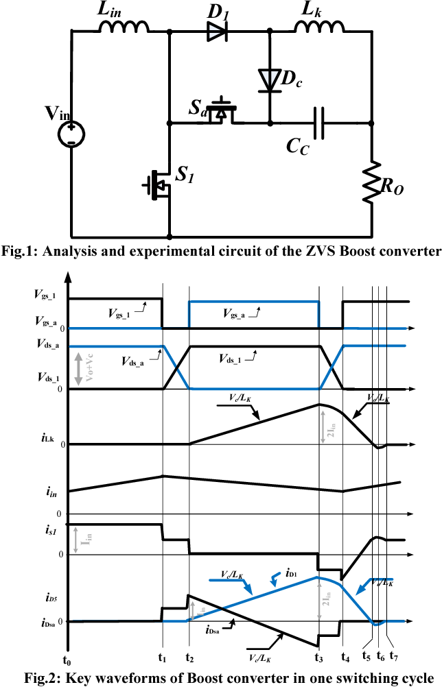
Assume V in 30 V and T s 10 s and the output current is at least 1 A. The active clamp boost converter ACBC has been analyzed and a complete model has been obtained. Design and Analysis of Soft-Switching Boost Converter.
Buy High Voltage DC-DC 8-32V Boost Converter 12V to 45V-390V ZVS Boost Module Capacitor Charging. In this converter an active clamp circuit is used to absorb the. The efficiency of the.
37 Full PDFs related to this paper. This is more useful than purely ZCS or - ZVS operation. Minimised if each switch in a converter utilises soft switching technique to change its status.
Initially an analysis of the electromagnetic processes in the power. The simulation was performed using PSpice software. Design modeling simulation and experimentation Nikolay R.
The technique of zero voltage switching is applicable to all switching topologies. It has been checked that it behaves as a voltage source with high input impedance. A boost converter step-up converter is a power converter with an output DC voltage greater than its input DC voltage.
Study and Design of a Zero Voltage Switched Boost Converter. 38 rows This reference design works as active clamped boost converter with ZVS. The design of multiphase converters.
This paper presents the design study of Zero-Voltage-Switching ZVS for resonant dcdc boost converter with M-type switch. Built based on the converter design and typically waveforms are presented to confirm the feasibility of the converter as well as computer simulation results. This presentation will focus on.
ZVS Resonant Converters 27 7 Chapter 6 Comparison Switching Techniques 32 8 Chapter 7. A quadratic boost converter is selected due to its capability of providing a wider voltage conversion ratio compared to the conventional boost converter for a given duty ratio d. The developed converter is applied to boost the output of a PV panel.
This paper presents the work of the new buck-boost converter that provides zero-voltage turnon and zero - current turnoff. 1a and was proposed in a similar form as a hard-switched converter in 10 which is referred to as tri-state boost converter and which allows to im-prove the dynamic performance of the converter by. Hinov In the paper work are shown results from researching of a single transistor Buck-Boost ZVS DC-DC Quasi-Resonant Converter.
A New ZVS-PWM Full-Bridge Boost Converter Mohammadjavad Baei The University of Western Ontario Supervisor. Through this process all the parameters values can. The buck regulator and its derivatives forward half and full bridge the flyback and boost converters to name a few.
Based on the proposed bridgeless boost rectifiers novel IBB converters can be derived by employing the input stage of an isolated buck converter as the primary-side circuit of the IBB converters. The design example specifications listed in Table 1 will be used for all of the equations calculations. This paper presents the design study of Zero-Voltage-Switching ZVS for resonant dcdc boost converter with M-type switch.
PFC boost converter design guide Application Note 4 Revision11 2016-02-22 Design Note DN 2013-01 V10 January 2013 2 Power stage design The following are the converter design and power losses equations for the CCM operated boost. Open image in new window. Up to 10 cash back In this paper a new non-isolated DC-DC converter is proposed.
Design and Analysis of Soft-Switching Boost Converter. A short summary of this paper. This converter topology is a high step-up boost converter with an extended voltage multiplier cell and a Cuk converter as a series output module.
In this study among the new class of ZC-ZVS PWM converters a quadratic boost converter adopting this technique is presented as an example. 2088-8694 ZVS Full Bridge Series Resonant Boost Converter with Series-Connected Transformer Mohamed Salem 815 The gain curves and the soft switching boundaries are shown in. I believe that single switch boost converters eg.
In a ZVS design due to the lack of the gate to drain Miller charge which is deleted when V equals zero. Because of this feature this topology is suitable for multiphase design where different stages share the load in a passive way without any extra mechanism or components. Throughout the study all parameters had been calculated in order to.
This is an important. Up to 10 cash back Design a ZVS buck-boost converter with the following steady-state operating point M 055 f ns 03 and Q 01. It is a class of switching-mode power supply SMPS containing at.
Figure 1 From A New Zvs Pwm Active Clamping Buck Boost Converter Semantic Scholar

Proposed Zvs Boost Converter Topology Download Scientific Diagram
Qsc Zvs Buck Boost Converter Operation A First Stage B Second Download Scientific Diagram

Buck Qr Converters A With Zcs B With Zvs Download Scientific Diagram

Final Year Power Electronics Projects Hpf Converter With Zvs Transition

Proposed Zvs Boost Converter Topology Download Scientific Diagram

Active Clamp Zvs Buck Converter Download Scientific Diagram

Zvs Three Level Boost Boost Converter With The Parameters Designed In Download Scientific Diagram
Arduino Dc Dc Boost Converter Design Circuit With Control Loop Mcuhq

Proposed Zvs Zcs Integrated Boost Converter Download Scientific Diagram

Zvs Quasi Resonant Boost Converter With Tapped Inductor Download Scientific Diagram

Zvs Boost Converter Mode 4 Download Scientific Diagram

Boost Converter With Auxiliary Circuit With Zvs Feature Download Scientific Diagram
A Dsp Based Digital Control Strategy For Zvs Bidirectional Buck Boost


Active Clamped Zvs Current Fed Full Bridge Dc Dc Converter Download Scientific Diagram

Lecture 6 Ch 6 Boost Buck Boost Zvs Pdf Eel6246 Power Electronics Ii Chapter 6 Lecture 6 Dr Sam Abdel Rahman Zvs Boost Converter The Quasi Resonant Course Hero
A 1 Mhz Zvs Boost Dc Dc Converter With Active Clamping Using Gan Power Transistors Semantic Scholar

Conventional Full Wave Zcs Qr Boost Topology Download Scientific Diagram

A Novel Zvs Zcs Boost Converter With An H Bridge Auxiliary Lcc Resonant Circuit Semantic Scholar
Posting Komentar untuk "Zvs Boost Converter Design"